The characterisation of materials and material systems is an essential aspect of materials science. A few decades ago it became obvious that, because the properties of materials depend so critically on the microstructure of their components, this characterisation must be determined to the atomic level. This means that the position – as well as the nature – of individual atoms has to be determined at “critical” regions close to defects such as dislocations, interfaces, and surfaces. The great impact of advanced transmission electron microscopy (TEM) techniques became apparent in the area of semiconducting materials, where the nature of internal interfaces between silicon and the corresponding silicides could be identified, and the results used to enhance the understanding of the properties of the compounds studied. At that time, advanced TEM techniques existed predominantly in the US. However, advanced TEM instrumentation was not available in the ma terials science and solid-state science communities in Germany. This gap was bridged by the late Peter Haasen who, after a visit to the US, initiated a Priority Programme on Microstructural Characterisation at the Volkswagen Foundation (Hannover). The programme was in effect from 1985 to 1997 and supported a wide range of research projects – from fundamental, trendy, innovative projects to projects in applied materials science.
“Gray’s Anatomy for Students Flash Cards 5th Edition” has been added to your cart. View cart
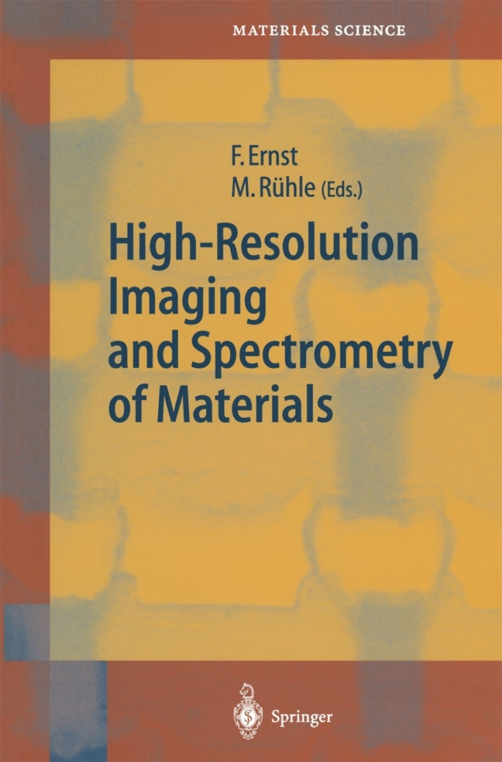
High-Resolution Imaging and Spectrometry of Materials 1st Edition
Author(s): Frank Ernst; ‎Manfred Rühle
Publisher: Springer
ISBN: 9783540418184
Edition: 1st Edition
$39,99
Delivery: This can be downloaded Immediately after purchasing.
Version: Only PDF Version.
Compatible Devices: Can be read on any device (Kindle, NOOK, Android/IOS devices, Windows, MAC)
Quality: High Quality. No missing contents. Printable
Recommended Software: Check here

